Sunday, September 25, 2016

A MFL inspection demo kit

Long ago in the distant land of late-semester grad school crunch time, an expeditious self-variant thought it was a good idea to voluntarily adopt a course project requiring research and fabrication of equipment.  While I can barely recall the scent of ambition, that physical device was one of its few remaining tangible products.  Let us go back in time for a moment...


With a cluster of retirements happening in the department at the time, I was in the last semesters of my MSc path with no choices for courses that would meet requirements.   After talking with one of the ME professors I'd been working with on a research project, I wound up surfing in a soft overview course on NDT methods.  As the only EE student in a ME course full of ME students, I felt compelled to take every opportunity to see if my own background could bring something fresh to the body of student work and discussion that took place. 

The last course project had quite a bit of latitude, but the basic idea involved a presentation based on a literature review, case study, or physical demonstration pertaining to a selected NDT/NDI method.  I opted to present and demonstrate a basic magnetic flux leakage (MFL) test.  While it would suffice to dig up some mothballed lab equipment and then make a PPT, I intended to make my own equipment and defect samples.  This was an opportunity to adopt an easy project that spanned a range of fun task areas.  It had everything from experimental component characterization, magnetostatic FEA, circuit design and simulation, programming, electronics fab, and machining.  I'd been burned out on project work in Excel and Simulink, and the chance at application and variety was appealing.

The concept of MFL testing is simple.  Local changes in the per-unit-length permeance of a sample can be detected by subjecting the workpiece to a static magnetizing field.  Near-surface flux is increased local to any defect which decreases the magnetic cross-section of the flux path.  All one needs is something to produce a magnetic field in the work, and something to sense the field near the surface.


While MFL sees more use in larger-scale applications and applications where the magnetics are purpose-built for particular surface geometry, my requirements meant I had a lot of latitude to make design choices that would otherwise make an impractical commercial product.  To make the equipment low-power and simple, I opted for permanent magnet excitation.  While this meant I didn't have the convenience of easily reducing excitation to ease manipulation or to suit different material thicknesses, I did incorporate the ability to incrementally add or remove magnets.  This makes the probe a bit difficult to use at times, but that's acceptable.

Since I'd been spending a lot of time doing magnetostatic sims in FEMM, I figured I'd play with it and get an idea of what I should expect.  With an approximate model, I could get an idea how much excitation I'd need for a given sample defect.  I could decide on pole and sample dimensions and I could figure out what the flux densities to expect at the sensor for a given selection of magnets. 


I figured the simplest way to sense near-surface leakage flux was to provide a shunt path through a hall effect sensor.  Some small steel pole pieces could serve as my low-reluctance path, and I picked a commutation sensor out of a small BLDC motor.  While I had plenty of these used sensors, they were all unidentifiable SMT parts for which I had no data.  I simply looked at the application I'd taken them out of and decided on a similar method of use.  In most of these 3-phase BLDC motor drive applications, the three sensors are driven in series from a fixed (5v) supply with a single series resistor.  The motor drive IC has three differential sense inputs and does everything else.
  

To characterize the sensor response to an applied field, I borrowed a disused magnetometer from storage at the physics department and set up a test fixture using a modified transformer frame.  Still using a simple series resistor and fixed voltage source, I set the sensor up with an excitation current equal to what it would have in its original application.  I placed the sensor and magnetometer probe in the middle of the fixed core gap and incrementally energized the device with DC.  If I hadn't been a dumbass at the time, I'd have realized that magnetoresistive effects meant that current was actually varying with flux density and possibly reducing response linearity.  While a current-regulated design might have benefits, I didn't think about it at the time.  I wasn't out to make absolute measurements of fields; all I needed were roughly linearized relative measurements.  For all I know, these sensors may have never been rated beyond 50mT or 100mT.  I took what I had and ran with it.


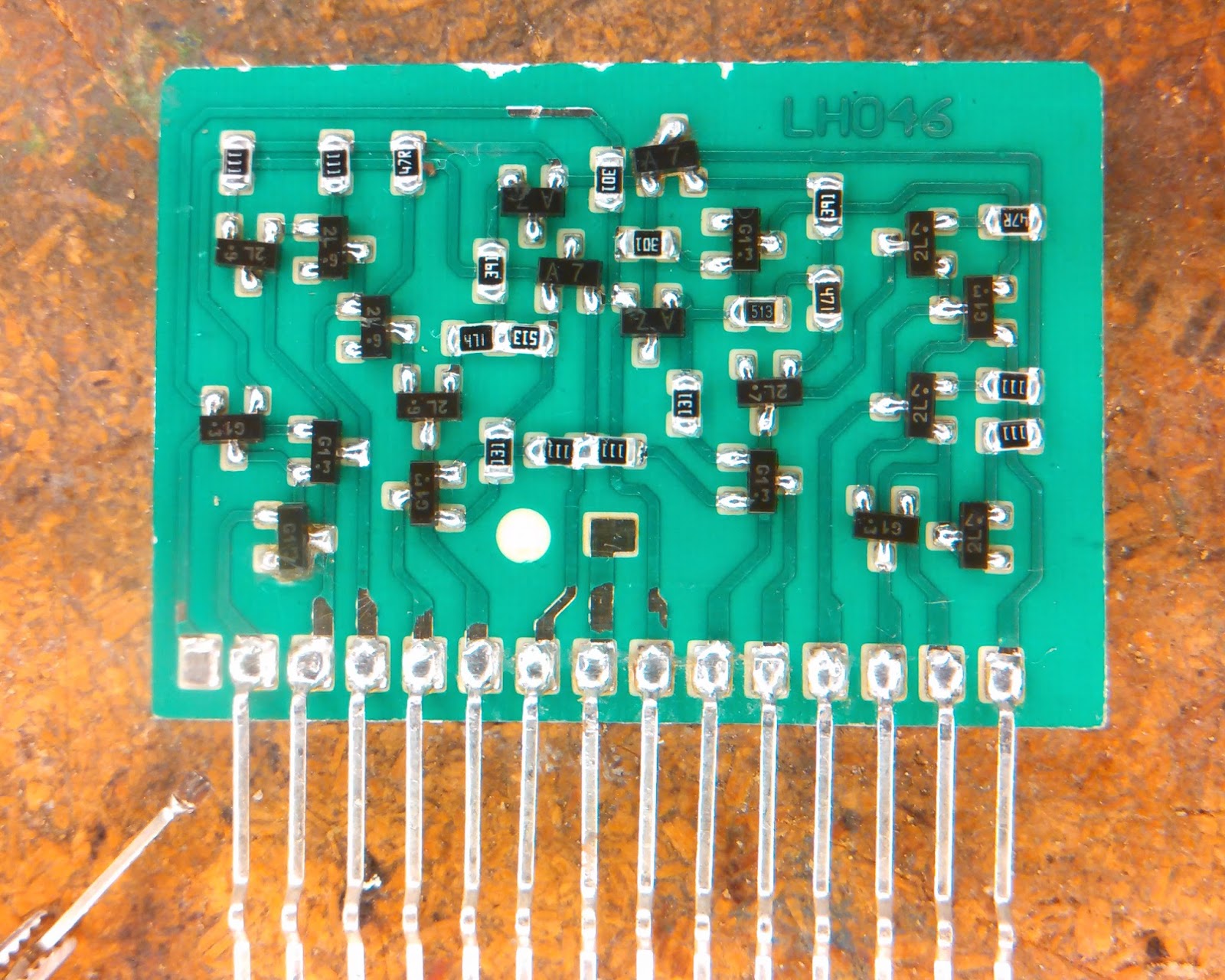
For sake of dirty simplicity, I made a LUT and configured an ATTiny25 microcontroller to sense the differential input and drive a meter via PWM.  I could have used a proper differential amplifier or even built a linearizing differential amplifier, but I didn't.  If I had used an instrumentation amplifier, I probably could have had the sensitivity to work with less magnetic excitation.  The microcontroller allows absolute reading of sensor flux density or it can be set into a convenient 'relative' mode where a baseline reading can be zeroed out.  This essentially stretches the scale and exaggerates meter movement when scanning an area.  Although I'm pretty sure I did a board layout for it, I ended up cobbling it together on nasty old perfboard from junk components.  The pot is for setting the meter range.  The meter is from an old rusted tacho/dwell meter I found on a scrap pile.  While the original face marked in RPM was coincidentally correct for reading in Gauss, I kept forgetting which of the multiple scales to use.  Also, fuck CGS units.  I simply made a new scale with tiny ass text so that I'd have something to squint at.


The probe was fabricated out of cold-rolled 1018 flat stock.  The straps are aluminum, and the shanks of the tie-bolts are unthreaded so as to help maintain total yoke permeance.  The sensor is soldered to a small bit of FR4 with a notch cut in it so that the narrow faces of the pole pieces can abut the sensor package directly.  


The sensor assembly is encapsulated in epoxy resin.  One of the yoke poles was lined with kapton tape so that it could be freed from the cured epoxy.  In this way, it can be pulled into alignment when the magnets are installed. Yes, that's an old PS/2 cord.


The operating faces of the yoke and sensor poles were all ground coplanar and then hand-lapped.  Although it was really unnecessary, I also dressed the top faces of the yoke poles and the shunt bar.  Everything is square with little chamfer, which makes it very uncomfortable to use considering how ridiculously strong it is. Due to their much higher intrinsic coercivity, NdFeB magnets don't really need a keeper shunt for the same reason an AlNiCo magnet would; still, it is needed to keep the probe's stray field from being a hazard to other equipment when it's not in use.  When dealing with thick plates, placing the probe or removing it from work surface can be made easier if the shunt is kept in place temporarily.  A design utilizing a diametrically-polarized cylinder magnet as in a switchable test indicator mount would obviate the need for a loose shunt bar, but It would complicate pole geometry, and i wasn't trying to make a marketable product.


The test sample was made from 1x1/4" 1018 bar and includes a slot, a set of flat-bottom holes, and simulated crack features made using rod to plug cross-drilled holes.  All these features are easily detected with the probe on the unmodified face of the bar.  Even the 1/16" deep FBH is clear as day when probed.


After presentation, I really had no use for the thing.  While I probably should have just donated it for class use, I ended up keeping it.  Occasionally, I'll use it to check the air compressor tank or something.  It's not really suited for measuring against curved surfaces, but it works well enough.  Probably the biggest issue is that I can't expect work geometries to be known or consistent.  Every test subject will be unique, and the most I can hope to find is a variation in permeance.  Without a chance to calibrate the process to a particular application profile and geometry, I can't really quantify much.

For sake of this blog post, I dragged an old air compressor tank off the scrap pile and mapped the bottom of the tank.  The paper acts as a positioning guide and it also allows the probe to slide more easily over surfaces without abrasion on rust or stiction against paint.  The map only covers one side of the tank because there's a weld seam on the other side of the centerline.  It's enough to make the point.  There's a 4" wide band of corrosion inside the tank, beyond which the leakage readings are almost constant save for variation caused by seating against a curved surface.


Of course, there are other ways to detect tank damage that's this bad.  In fact, the change in permeance is large enough that it can be detected by sliding a similarly strong magnet along the surface and feeling the change in attraction force.  Of course, it would have to be a strong pot magnet or something designed to make a closed low-reluctance flux path.

Maybe someday I'll come up with a cool job for it to do.  Until then, I guess this is about all the glory it'll get.

Wednesday, September 21, 2016

TV, LAN, & intercom over one cable

The buildings on this property have shared a single MATV system installed several years ago.  This consists of two long RG11 drops and sundry splitters, taps, and amplifiers.  Over the years, the system structure has changed several times.  For many years before DTV conversion, music and security camera feeds were inserted into the network with modulators.  Slowly, the modulators and processors were removed and all that remained was a simple antenna distribution system.

Property & Drop Map

The off-air TV/FM signal isn't the only thing shared between the buildings in the diagram.  While the antenna is distributed from building A, the WAN connection is at building B.  For years, building A has been linked to the computer network over wifi with the aid of directional antennas.  Furthermore, buildings B and C share a voice intercom I'd discussed in a previous post.  This intercom was realized using a parallel drop of twisted pair cable.  The recent goals were to extend the computer network to point C and to replace the deteriorated UTP cable used by the intercom.

Network schematic between buildings B and C

While the wireless bridge to A works well enough, reaching C via wifi is difficult.  There is restricted line of sight and the obstacles in the signal path are all large metal structures.  While the 500' link can be established with makeshift waveguide antennas, I opted to try running it over the coaxial cable instead.  While I'm sure there are legitimate solutions for running ethernet over coax, the products I saw were either too expensive or appeared to be misrepresented Thinnet adapters.

https://www.asus.com/us/Networking/RTN12_D1/ 
http://www.hollandelectronics.com/catalog/upload_file/DPD2.pdf

Like usual, I used a low-cost and low-risk approach.  Parts should be inexpensive, common, and should have some secondary utility should plans change.  Using two ASUS RT-N12/D1 router/repeater/AP devices, a 802.11g/n link was made over the coax.  Satellite diplexers are used to combine/split the 2.4GHz signal from the MATV signal.  I made a simple adapter to connect the RP-SMA antenna port on the AP to the 75 ohm network.  The adapter serves to adapt the dissimilar connectors, but it also uses a simple L-pad impedance matching network and a single capacitor as a DC block.  The odd resistor values shown in the schematic are a product of convenience given my limited stock of SMD resistors.  Simply put, 100R || 1K = 91R; 75R || 100R = 43R. I gutted some old CATV channel traps to use as enclosures.  The RG316 cables with RP-SMA connector were stripped from old equipment.  Signal strength at C is about -57dBm, which is about on par with what can be expected of the drop.  The free antenna on the access point at B provides extended coverage to the shop and outdoor area.  The free antenna on the access point at C provides wireless coverage for any mobile devices in the area. 

Inner strand damage caused by jacket cracking in UTP cable

The UTP drop used by the intercom was originally a bundle of scrap indoor cable pulled from a PBX somewhere.  It was never expected to last outdoors for as long as it did.  Eventually, the jacket deteriorated and the cable would become waterlogged.  Due to the way the intercom is arranged, shunt conductance in the line does more than attenuate the voice signal; it causes the intercom to ring incessantly when on-hook.  Numerous modifications were made to the previously detailed intercom in order to make it robust against these faults, but ultimately it's difficult to work with a line that has roughly 1 ohm shunt resistance when it rains

http://sonorastore.com/500.html

The voice intercom project followed a similar course.  Two power inserters were used as diplexers to couple the voice and DC from the intercom.  Again, as a matter of physical and electrical interfacing, I made a pair of low-pass filters with screw terminals to attach to the indoor portion of the intercom network.  I felt that adding the LPF was prudent, as the DC path of the power inserters has a cutoff frequency of a few MHz.  I didn't want stray RF interfering with anything.  The LPF knee is set at about 20kHz, but in reality, it doesn't really matter so long as it encompasses the ~3.5kHz voice band allowed by the old telephone hardware.  There are versions of these power inserters with additional DC port LPF filtering, but I have no idea what the cutoff frequency actually is.  These may be an option and may avoid the need for external filters, but as with most things, if you're out to apply a product for an off-label use, you're going to have to perform some experiments. 

LPF filters for intercom connection

It's worth noting that this change means that the intercom signal path is now sensitive to ground loops, whereas before the remote end of the UTP was floating.  Attention has to be paid to grounding within the intercom base station and on the coax drop.  In my installation, the DC side of the base station's power supply is floating.  The coaxial drop has a hard ground at only one end.  The far end at C is grounded through a TVSS diode.  This breaks the ground loop created by the shield, but allows any surge currents to shunt to ground.  I imagine two antiparallel diodes would work just fine as well. When all ground loops are opened, the intercom is remarkably clearer over the coaxial drop than it ever was over UTP. 

Drop feed at B showing diplexers, fabricated adapters, and ground block
While the power inserters and diplexers are being used marginally beyond their specified bandwidth, they work well enough; after all, most of the fittings in the 2.4GHz path were only rated to 1GHz until the last few days. The components for this approach are inexpensive and easily obtainable.  The details of the adapter construction are not terribly critical.  It all works with an ugly simplicity that impresses me.

Saturday, September 10, 2016

Casual Amusement With a RSN311W64

While I was waiting on parts to repair my Marantz, I decided to scrap out a number of accumulated bits of equipment and loose PCB's.  One of these items was a 2000-era Panasonic surround receiver with DVD player.  I'd pulled it from service after it had slowly lost all audio output.

Panasonic SA-HT80

When I had first pulled it, I had intended to repair it.  Upon opening the case and seeing heat damage to the paper-phenolic PCB around essentially every semiconductor, I decided it wasn't going to be worth the effort.  I never bothered taking photos at the time, but disassembly was no longer possible without destroying things.  The board interconnects were so stiff that the damaged PCB's broke apart like crackers.  I amused myself by nudging transistors out of their fractured solder joints or peeling traces.  I pulled a large selection of capacitors from the board.  Out of about 50 capacitors, about 4 or 5 were not bad.  Almost all were less than half their original capacitance or had ESR > 50 ohms.  This included small electrolytics in areas of the chassis that were never abnormally hot.  I don't think I've ever run across a piece of equipment that managed to degrade so completely and uniformly without any catastrophic failure.

Totally not my photo

I kept the transformer and I pulled the generic-looking RSN311W64 amplifier hybrid for later.  That was then, so I guess this is later.  Since I was pleased with my attempts to photograph the STK3122 in the last post, I figured I'd pull out the phone and fight autofocus for a half hour and get some half-blurry pictures.


Let's pretend it's artistic.  If you aren't afraid of translating things, there are other dissections out there that had the benefit of more suitable tools.

As a bonus, I disassembled a Motorola SRF397 transistor and took a couple pictures.  It's not terrible considering it's handheld photography with a phone.


Thursday, September 1, 2016

Exploring the Sanyo STK3122-III

As part of my routine management of perpetually failing appliances, I once again found myself repairing my Marantz TA170AV.  Fully suspecting the failure, and recalling that I'd mentioned it in passing once before, I figured I would approach the repair with a mind to be a bit more analytical.


This receiver came to me years ago after suffering a slow degradation of output power over the course of months.  The original owner endured the loss of one channel and then the next before gifting it to me in the traditional manner.  What better way to reduce the regret of discarding a failed investment in equipment than to let it disappear into the life of that techno-hobo friend of yours? At the time, I merely traced out the signal path and found that the STK3122 amplifier module was dead.  I replaced it with a part from a repair shop, and all was well.


The unit sat unused for nearly a decade before I dragged it out and put it into service.  After about a year or so of mild use, I began to get noise in one channel intermittently.  The noise would follow in the wake of salient bass excursions, almost like a bad volume pot, speaker switch or other poor connection.  I frustrated myself with trying to fix connections before I noticed the crossover distortion getting significantly worse.  At that point, I pulled the unit apart and checked the biasing.  Sure enough, the STK3122 was at fault again.

In the course of looking for a replacement, I began to question what I should expect.  I know that counterfeit parts exist, and I had bought the replacement from a domestic brick & mortar store, so I assumed I was in possession of two vintage modules which had failed in nominal operation.  Was there some issue with device degradation over time (metallurgical, thermomechanical, or environmental factors) which would make vintage parts inclined to be less reliable?  I bought two replacements: one was a used vintage part, and one appears to be a NOS vintage part.  Once more, I replaced the module and everything worked.

Out of curiosity, I decided to see if there was anything to be seen inside the module packaging.  The datasheet provides an internal schematic, so maybe if there were indications of a failure cause, there may be an indication of what to expect of replacement part reliability.

Note lead width and exposed substrate insulation near pin 16

Starting with the original part I'd stripped from the unit years ago, I simply used a spudger and a lacquer thinner bath to remove the nylon device cover and reveal a beautiful hybrid circuit consisting of wire-bonded bare dice and printed film resistors.  I traced out the circuit and matched it to the schematic.  It's interesting to note that this layout includes the 470 ohm resistors and pads for capacitors which would allow the external compensation networks described in the datasheet test circuit to be built internally.  I'm not sure if there was ever a family of part cousins which made use of these internal features. 


As can be seen, the bias resistors R9/R18 appear to be scratched.  On closer inspection, both resistors were open-circuit.  The top silkscreen layer over the resistive material has multiple fine cracks across it, and the conductive material is broken along two narrow cracks which show evidence of local heating.  Assuming no external circuit factors could induce this within the scope of its rated bias point, this suggests any number of things that could be at play.  Quiescent power dissipation of the package is on the order of 3W.  These things run fairly hot without a heat sink.  The observed cracks could merely be a cumulative effect of heat causing material shrinkage or degradation in a static sense.  The dynamic effect of substrate expansion could also stress these resistors.  Once cracks begin to form in the conductive printing, current crowding at the partial connection will only result in localization of resistor power dissipation and further localization of its degradation.


That's my theory anyway.  I still had a second part to dissect.  Unlike the first one which had two completely dead channels, the recent failure had one good channel and a partially failed channel.  I was hoping to be able to compare the results and see if I could determine the original value of R9 and R18.  Maybe I could even demonstrate a repair!

Note lead profiles and lack of substrate connection
After some soaking and picking and prying, I eventually got the second module apart.  Much to my surprise, it had been a counterfeit part all along.  The entire module is constructed from SMT chip resistors and SOT-23-3 parts.  Obviously, none of this will help us determine part values in a legitimate Sanyo part.  In the process of disassembly, I had noticed that the leads seemed terribly easy to bend.  When I had tested this module in a breakout board, I had similar issues. Before long, the leads started peeling off, revealing the dark copper underneath.  Most of the leads on the part show similar signs of plating/solder failure.  I am not sure that this isn't the only thing wrong with the part.  The part had demonstrated faulty output bias when in-circuit, but my tests with the part on a breakout board were varied.  If I weren't lazy and worried about abusing the receiver's PCB, I'd fix the leads and reinstall it for a test. 

More delaminated leads
I need to emphasize what pictures like this reveal.  What you're looking at are copper leads which are mechanically socketed into form-fitting solder fillets, but not necessarily electrically connected to them.  The electrical continuity between the soldered areas on the PCB and the component MCPCB may be made via intermittent semiconductive contact between copper oxides and/or intermetallics, or it may be relying on the cross sectional area of the plating alone.  Just because the leads don't wiggle around and fall off doesn't mean a reliable electrical connection exists.

The schematic of the fake is identical to that shown in the original datasheet, though all the values are different.  All PNP transistors are MMBT5401 parts; all NPN transistors are MMBT5551 parts.  These are rather common general purpose 160v transistors.  The diode pairs are BAV99 parts.  It's noteworthy that all the parts in the counterfeit could easily be replaced.


I had to question how this handful of 0805 chips and SOT23 packages can comfortably dissipate a total of 3W.  For the moment, let's disregard the MCPCB and try a sanity check.  Assuming a limiting dissipation of 200mW per part, the module could dissipate >7W.  Of course, power isn't dissipated across all components equally.  I decided to take a look at the circuit and see if I couldn't come up with a better idea of the distribution of power in steady state.

I recreated a single channel in LTSpice and set an approximate bias point by adjustment of a dummy load with null input.  When the dummy load sets the output differential voltage to match the application schematic, the total channel dissipation matches the observed dissipation of the module. Checking the estimated component dissipation, a few things of note stick out.  Q1, Q2, and their counterparts in the other channel are operating around 80mW.  Output transistors Q7, Q8 and the counterparts are operating at around 400mW.  R9 and R18 are dissipating about 300mW each.


Keep in mind that this is just a halfass simulation with a simplified equivalent external circuit.  I fully accept that this could be inaccurate, but it falls in line with what would be expected.  Q7, Q8, and their counterparts will be the transistors with the highest dissipation.  The physical construction of the genuine hybrid part suggests this, and it's not like we can expect transistors like Q3, Q4 to contribute any significant fraction to the observed module power.

Considering Rth(j-s) values published for 0805 chips on multilayer PCB's with ground planes, 300mW on R9 and R18 doesn't seem too terrible.  The MCPCB should give these parts a lot more headroom than the worst-case values (~125mW) on a datasheet.  Then again, we have no idea what sort of value drift will occur.  The parts on the disassembled module are well within tolerance still.

Assuming it's an accurate estimation, the high dissipation on the output transistors might be of more concern.  Nominal power rating for these devices is going to be somewhere around 350mW.  This assumes minimal traces and pcb thermal conductivity.  Without a thermal resistance model for devices on a MCPCB, I simply assumed the substrate temperature is constant at 70dC.  This is higher than the observed temperature when operating without a heat sink.  Using a figure of 130K/W for Rj-c and a handwavy 10K/W for Rc-b, maximum allowable power within a 150dC junction temperature limit is somewhere around 600mW.  This is only a bit more than the highest figures for allowable package dissipation on multilayer boards.  These parts may be fine operating at 400mW, especially if the substrate has a heat sink attached. 

Of course, the thermal analysis says nothing about whether the counterfeit circuit can meet its specs in terms of noise, distortion, etc.  Although I may revisit it, I haven't bothered with much component-level testing of the fake.  I could put together a power supply and see if the quiescent dissipation follows the estimation.  I could pull the transistors in question and test them off-board to make sure they haven't been destroyed.  I may update this if I do anything more, but I'm inclined to believe that the fake was simply suffering from contact issues at the lead terminations.

While dissecting the fake doesn't help us better understand the original Sanyo part's internals, it does offer some information that will help make counterfeits identifiable.  There may be more than one breed of counterfeit out there, but I have been able to identify current Ebay listings which match this particular type. Also, this forum thread features the dissection of a fake STK3102 which matches these indicators.
  • The counterfeit appears to have a facility to allow pin 8 to be bonded to the aluminum substrate, although in the example I have, there is no substrate connection at all.  Counterfeit parts may lack continuity between pin 8 and the aluminum substrate.
  • The leads of the original Sanyo part are an iron alloy (magnetic), whereas the counterfeit leads are nonmagnetic. 
  • The original leads also have a sheared shoulder near the package connection.  In the photos, it's easy to see that the leads are slightly wider near the bend.  The leads on the counterfeit are formed differently and have a uniform width.  
  • It's also worth noting that any legitimately NOS parts will likely have heavily tarnished lead plating.  It's not a sure thing, but shiny beautiful leads are an indicator.  If you're buying a pulled part, who knows what kind of shape the leads will be in.
  • The orange substrate insulation of the genuine part is visible through the lead apertures in the molded plastic shell.  This is particularly easy to see in the empty opening for pin 16.  The counterfeit part is just a MCPCB and simply shows bright green solder mask everywhere. 
  • Finally, the easy way to spot some fakes is as simple as looking at the date/lot code on the front of the part.  The counterfeit part I disassembled has a code 5302.  Checking Ebay, I can find at least two "Genuine Vintage NOS" parts which have green solder mask, shiny leads, and a 5302 date code.
Ultimately, it's up to you whether the counterfeit parts are worthwhile.  Like I've commented before, I'm not against inexpensive parts in general, but if the part can't be trusted to meet its implicit specifications, its utility is severely limited.  I'm wary of the allowable power dissipation of the MCPCBA-type counterfeits, but I'm also worried about thermomechanical stresses in genuine hybrid parts.  In either case, I do suggest using a mechanically-supported heat sink on these parts.